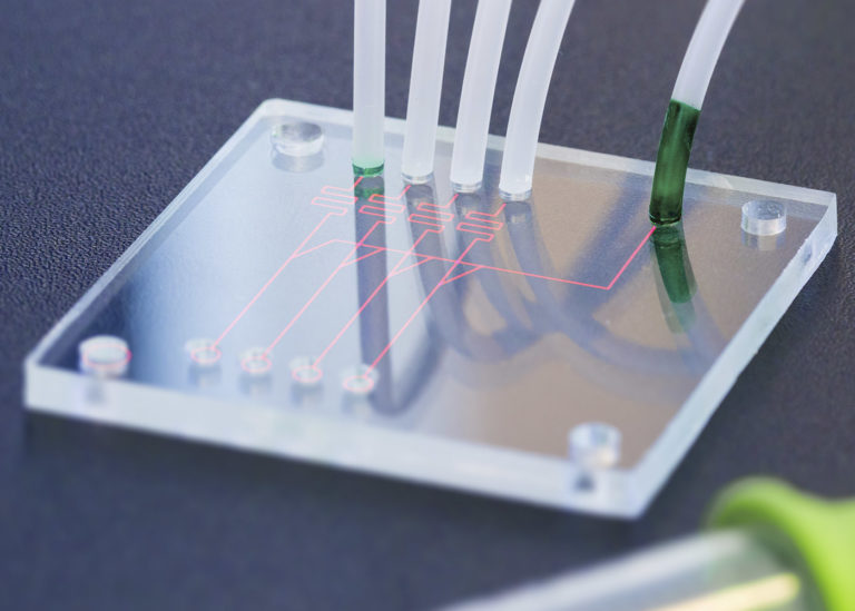
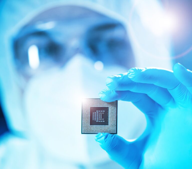

Maximizing Droplet Motion for Microfluidics Applications
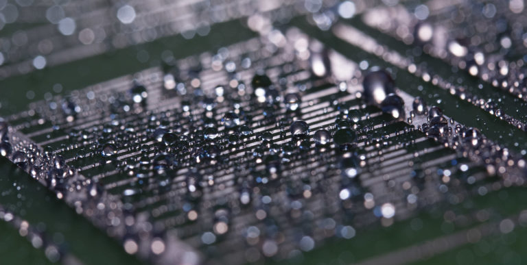
Electrowetting has emerged as one of the most commonly used techniques for manipulating the movement of small liquid droplets on surfaces, utilized in lab-on-a-chip devices, optics, and displays. It is achieved via electromechanical reduction of a liquid’s contact angle with an applied electric field on a solid surface. An electrowetting material system will typically consist of two coating layers – an insulative, dielectric coating layer, necessary to prevent electrolysis, followed by a layer of a highly hydrophobic material with low contact angle hysteresis.
Similar to most of the legacy coating solutions, GVD employs a multilayer approach to electrowetting, separating the dielectric and hydrophobic functions between two distinct materials. The difference lies in several significant improvements over one of the most common and successful combinations to-date, such as parylene C as the dielectric, and Cytop or Fluoropel as the hydrophobic layer.
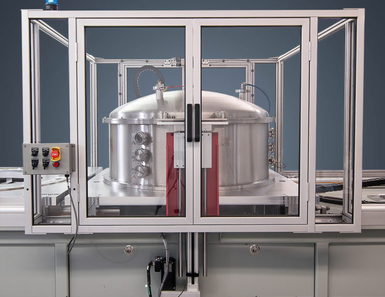
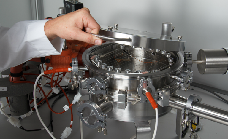
By contrast, both coatings in GVD’s electrowetting material system are vapor-deposited, ensuring ultra-thin, pinhole-free and uniform films. Chemical vapor deposition (CVD) is a dry, solvent and surfactant-free process that does not require annealing or curing; coatings are deposited directly on the surface of the substrate from the vapor phase, and polymerize in-place. A single-step deposition, without the use of harsh solvents or surfactants, results in uniform and conformal layers that do not plug small cavities and features. This material deposition method is especially ideal for applications that require consistent, reproducible films without adverse wetting effects or pinholes.
The high dielectric strength of the insulative, siloxane material allows for impressive thickness optimization. Depending on the application, it can be applied on the order of tens or hundreds of nanometers, allowing for minimum actuation voltage, wherever optimization is possible. The dielectric film can be applied over a wide variety of materials, and will maintain its superior adhesion throughout the life cycle of the device.
Similarly, the CVD hydrophobic layer does not exhibit the typical challenges associated with typical, widely-available fluoropolymers, such as poor or inconsistent coverage, pinholes or non-uniformity associated with wet-applied mode of application. Just like the base dielectric layer, the fluoropolymer used in GVD’s electrowetting coating system is transparent, and UV-stable. To further minimize hysteresis and reduce pinning, an optional (but highly recommended) post-processing step is used to maximize the favorable properties of the hydrophobic layer.
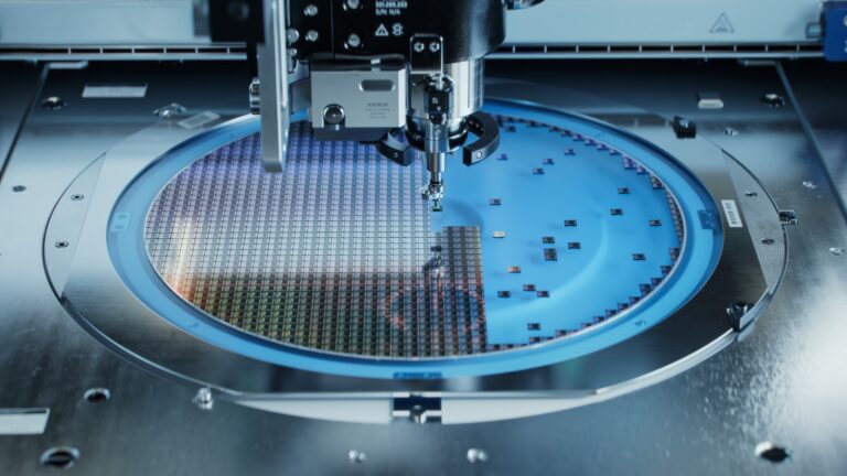
Most importantly, GVD coatings are scalable due to the nature of the deposition process, where batches of product can be processed simultaneously in one or more chambers, depending on the throughput required. CVD processes are generally recipe-driven, and are thus highly reproducible and repeatable.
Due to its unique set of benefits, GVD’s electrowetting material system is currently being explored for a number of cutting-edge applications ranging from DNA sequencing and preparation, drug discovery and molecular diagnostics.